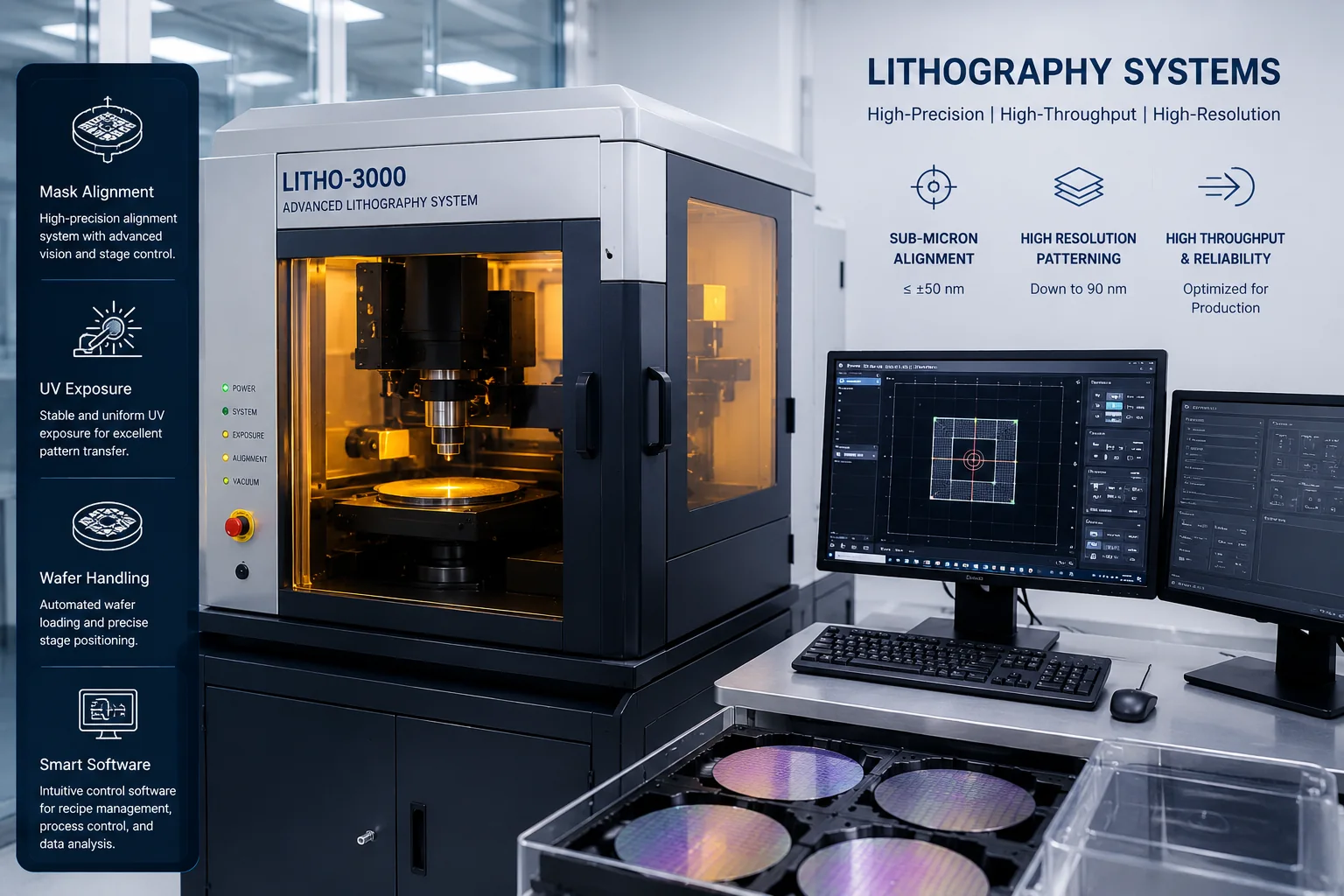
Advanced photolithography and mask alignment solutions for microfabrication and semiconductor patterning applications.
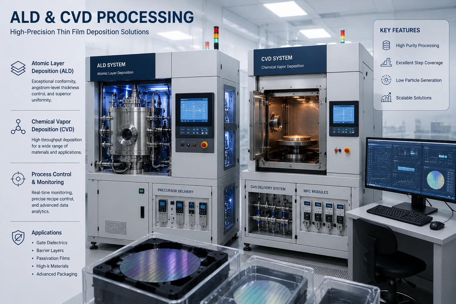
Atomic Layer Deposition (ALD) and Chemical Vapor Deposition (CVD) systems for high-precision thin-film fabrication.
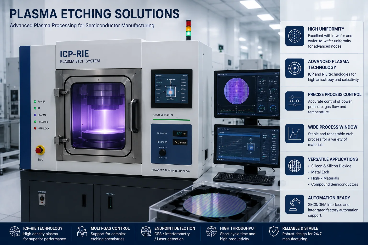
Reactive ion etching (RIE), ICP etching, and plasma processing platforms for semiconductor manufacturing workflows.