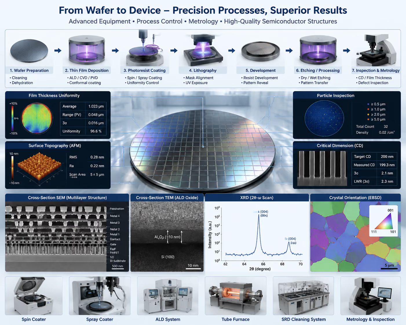
Advanced photolithography and mask alignment solutions for microfabrication and semiconductor patterning applications.


We specialize in supporting research laboratories, universities, research institutes, and technology development centers working in semiconductor science, microelectronics, photonics, advanced materials, and nanotechnology.
Our focus is not large-scale mass production, but rather the development of research infrastructure and experimental platforms that enable scientists and engineers to explore new materials, optimize fabrication processes, and validate emerging technologies.
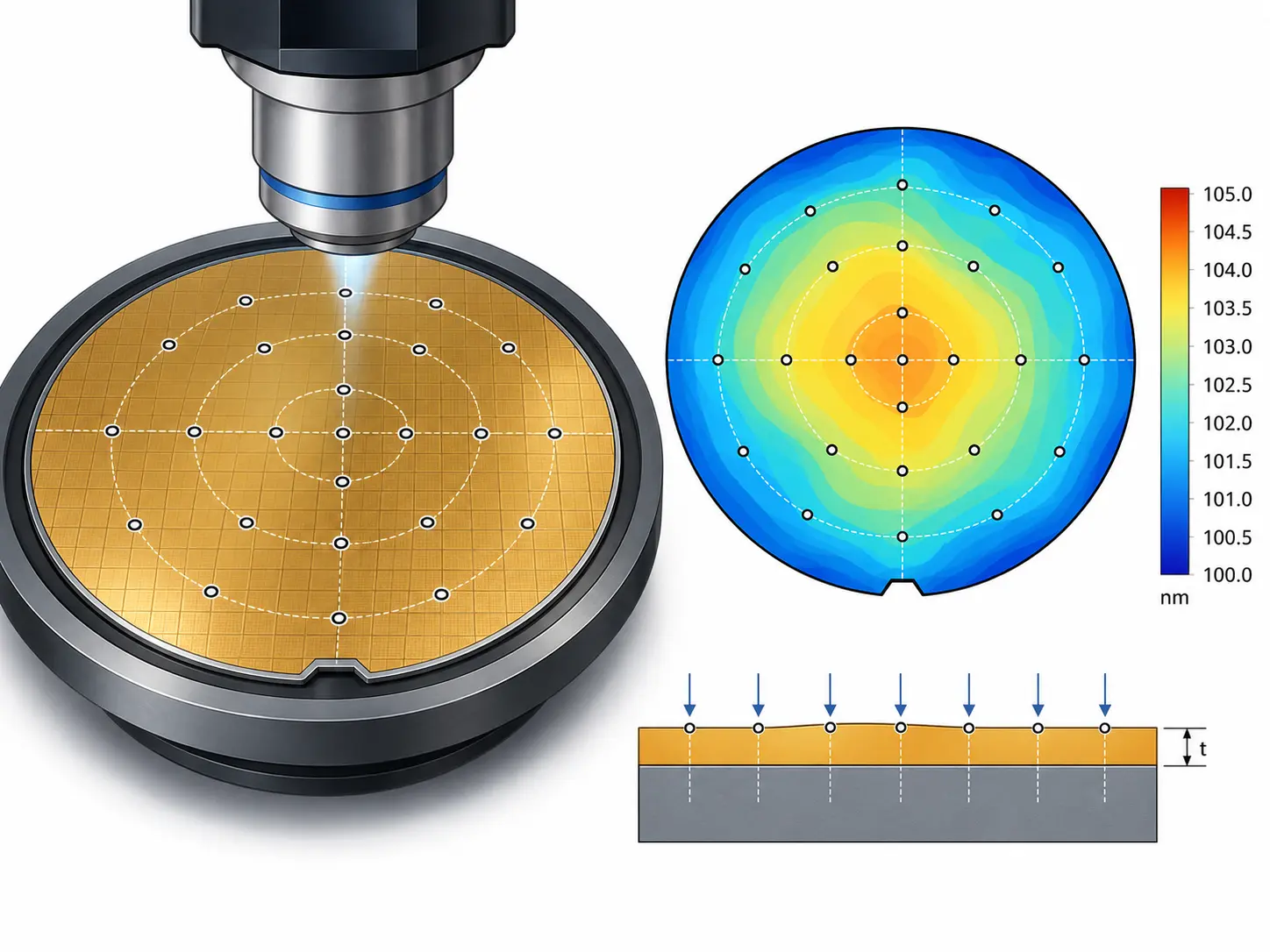
We provide equipment, materials, and engineering support for every stage of semiconductor research and process development — from substrate preparation and thin-film deposition to lithography, thermal processing, characterization, and device testing. Whether establishing a new laboratory, upgrading an existing facility, or expanding research capabilities, we help organizations build complete and efficient experimental environments tailored to their specific applications.
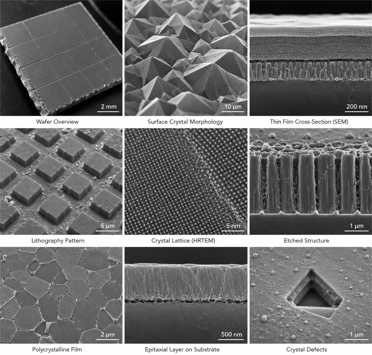
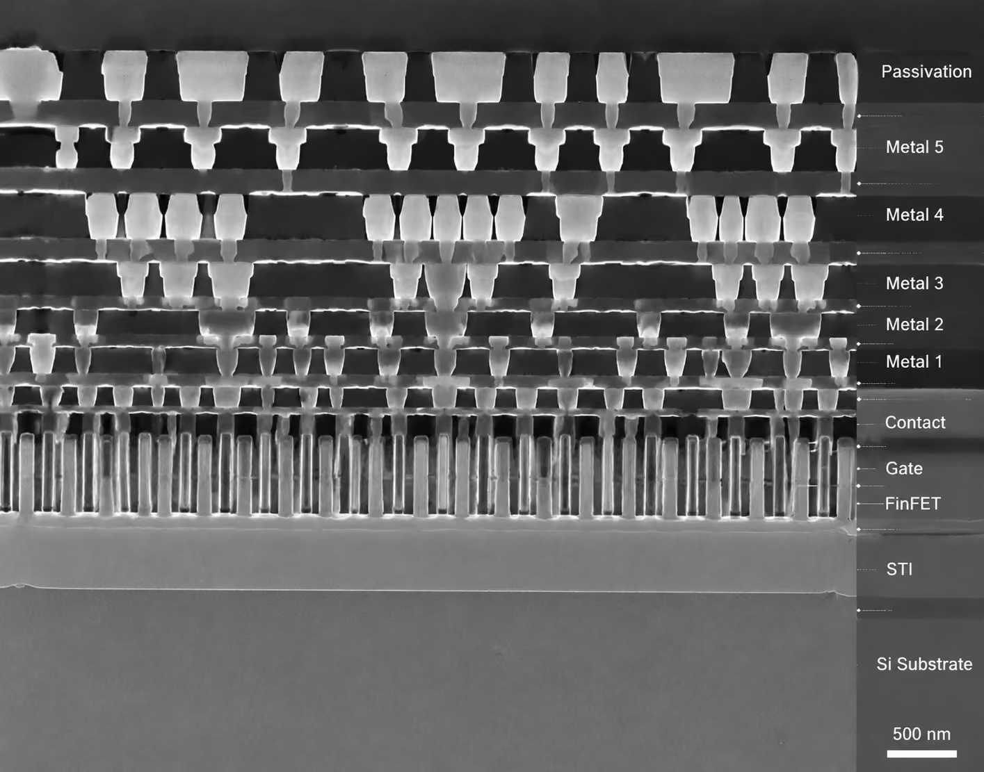
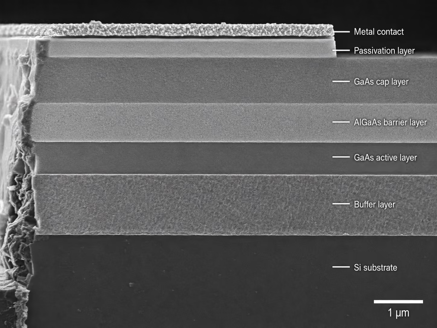
Typical results include epitaxial crystal growth, thin-film deposition, micro- and nanostructure fabrication, and semiconductor material development.